SAS PCB
Where Quality Meets Innovation in PCB Assembly
PCB Design For Manufacturing (DFM) Tips
Tip 04:
Concise Silk Screen
What is a silk screen/silk screening?
On a printed circuit board the silkscreen is a process whereby a layer of ink is traced and applied. This is usually used to make it easy for manufacturers and engineers to identify individual components as well as show marks, logos, symbols and any other information that may need to be marked on the PCB.
Usually, a non-conductive epoxy ink is used. It is formulated differently than regular printing ink. The most common colour is white but yellow and black can also be used.
What kind of information should a silkscreen be used for?
It can be used to convey any important information but in general it is to help someone:
- Understand any dangers or warnings.
- Polarity of individual components.
- Find test points or an individual test point.
- Find individual parts or components by marking them with their reference designator.
- Add any unique identifiers to the printed circuit board.
- Add any manufacturer marks, version numbers or regulatory marks.
What is a silk screen/silk screening?
A clear and concise silk screen is very useful in the low/medium volume PCB manufacture process. Although placement and inspection is automated, humans operate and program those machines so a clear indication on the silkscreen is always useful.
Components can be supplied in the incorrect orientations and components can flip and rotate during placement.
SMT operators are all always looking out for issues both during and after a PCB assembly is being manufactured, a clear silkscreen can help them to identity errors quickly.
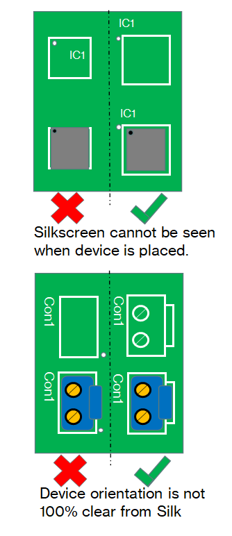
Keep your pin 1 orientation markings concise and keep them from being obscured by the components, a marking is no use if it's under the device.
Ensure the Silkscreen represents the device that is fitted, often a silk screen image of a connector is far more reliable than a pin 1 marking.
Misunderstandings can be easily avoided if silkscreens are clear and look like the device being fitted.
Be careful of LEDs, often red LEDs can be anode marked, if you can make this clear on the silkscreen it will be forever remembered.
Ensure that the silkscreen on bottom termination/QFN type devices is clear of the component, they are designed to sit flat to the PCB assembly so if the silkscreen is under the device it can lift it and affect the solder joints.
What methods are used for silk screening?
The easiest method is Manual screen printing, this involves using a stencil comprising of the silk screen design whereby the ink is directed though the stencil and on to the PCB.
Another method used is Liquid Photo Imaging, this method is very similar to solder masking but instead of solder the laminate is coated with the epoxy based ink and then cured under UV light.
The other method that is used is direct legend printing. This is the most expensive method but allows for more complicated silk screening. It involves using an inkjet projector to apply the epoxy based ink and then just like the photo imaging process the board is then run under a UV light for curing.

Do You Like What You See?
Join the ranks of satisfied engineers and businesses. Register and quote today!
Register