SAS PCB
Where Quality Meets Innovation in PCB Assembly
PCB Design For Manufacturing (DFM) Tips
Tip 02:
Importance of Panel Borders
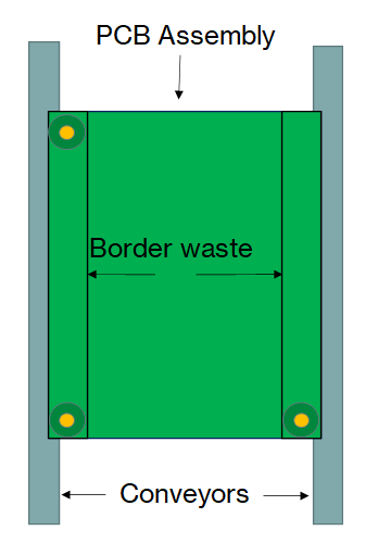
What are Panel Borders?
When it comes to producing a quantity of PCBs; instead of manufacturing a load of single printed circuit boards. What most manufacturers will do is project the printed circuit board design on to a panel that when finished will be contain multiples of the same PCB design.
The Panel Border is not part of the actual printed circuit board design. It is where extra material is added around the printed circuit board and is done in order to maintain mechanical stability of the printed circuit board or panel during assembly.
Why are Panel Borders Important?
Most production machines, paste printers, pick and place machines, optical inspection equipment selective solder machines, wave-solder machines, transfer conveyors, etc. cannot process boards less than a certain size so having edges and/or boarders alleviates this issue.
Most PCB assembly machines have conveyors and require unpopulated areas of PCB waste material for the purpose of traction when transferring PCB assemblies between different processes.
Having components too close to conveyors can cause them to be become damaged during transfer.
There should be no copper elements or holes placed right up to the panel border edges.
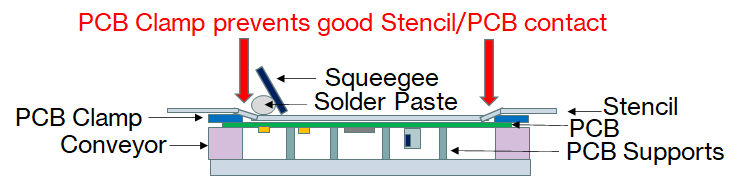
It's also important for the solder paste printing process that SMT component footprints are away from conveyor clamps.
The paste screen stencil will be forced away from the PCB at the edges of the conveyor clamps causing a poor paste screen gasket which can lead to a poor print.
SAS Ltd prefers a 10mm panel/PCB borders this allows for plenty of waste material to buffer against damage or poor paste screen gasket and makes no difference to cost in low volume.
Higher volume manufacturers often reduce the panel borders to the minimum required by their equipment to improve usage of FR4.
When you are designing a PCB for a panel it is important to keep Mechanical Stability and overall Panel strength in mind to avoid both damage to assembled PCBs occurring and/or warping. This is because as outlined previously the panel will be moved through various manufacture and assembly processes; some of which will involve high temperatures.
When it comes to Mechanical Stability something else to consider is component weight and distribution. If heavy components are part of the PCB this can cause mechanical instability however adding extra material to each PCB on your panel will help to alleviate this problem.
It is also important to consider components that overlap the PCB board edge, you should think about adding more clearance between PCBs in this case. This will allow these components to be fitted more easily and therefore introduce less problems which should also translate to better assembly yields.
It is recommended due to the physical characteristics of electroplated materials that copper distribution is uniform across the PCB/Panel. As a result sometimes a copper grid or extra copper may need to be added. This method is also good for ensuring mechanical stability as more copper will result in a more stable board with a lower chance of warping and flexing.
Do You Like What You See?
Join the ranks of satisfied engineers and businesses. Register and quote today!
Register