SAS PCB
Where Quality Meets Innovation in PCB Assembly
PCB Design For Manufacturing (DFM) Tips
Tip 05:
Trace and Pad Design
What are tracks?
On a Printed Circuit Board; the tracks (also called traces) are the conductive paths used to connect between each point on the board. Tracks can have different widths depending on the current requirements that they are required to carry.
When dealing with high frequencies it is important to calculate the proper track width so that the track has the proper impedance required for connecting the required components. You may also need to take in to consideration whether or not any of your components are sensitive to cross talk which will usually be mentioned on a components data sheet however for most components this will probably not be an issue.
What are pads?
A pad is a small copper surface on a PCB that has two main purposes, the first one is to mechanically hold component legs or pints and the second one; is to provide a point to hold the component on to the board using solder and provide connectivity to the tracks/traces.
There are two types of Pads. Through Hole pads are intended for attaching components with pins or legs so that they can be soldered from the opposite side. This is the more traditional way that components are attached to a board.
SMD or surface mount Pads are intended for use with Surface Mount Devices, rather than using longer pins/legs that are soldered from the opposite side surface mount components are soldered on to the same surface of which they are placed.
Plated holes are sometimes also used instead of pads, these are known as Full track or Through Hole VIAs (or Vertical Interconnect Access) and are used when an interconnect must instead go through to the opposite side of the board.
VIAs can be through hole whereby they go all the way through the board, blind where they go from one out layer into the middle of the board or buried where they are not visible externally but are present for vertically connecting one or more layers together.
What considerations should I make when desinging track/pad layout?
Remember It's important to consider trace/track and Pad layout especially on fine pitch devices, QFNs, BGA's or bottom termination devices.
Remember to always check advice from a given component's data sheet, often when problems are experienced in PCB manufacturing it's because a design rule or specification that is required for a component to function or be correctly placed has been overlooked.
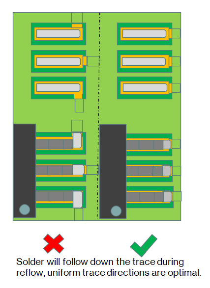
If you can; it's best to keep trace direction uniform so solder tracks away in the same direction from component leads during reflow.
Fine pitch bottom termination devices such as QFNs are sensitive to poor pad uniformity and inconsistent solder mask apertures, inconsistency can lead to poor assembly yield.
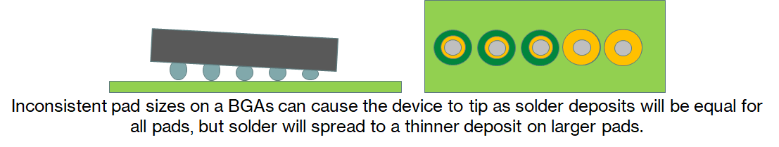
BGA's can also be affected by inconsistent pad sizes, this can lead to varying shapes of solder deposits under the device.
As mentioned above don't forget to check the datasheet and calculate the correct track width if using a component that requires a certain impedance.
It's best to keep the size of pad as consistent as possible under the device.
Do You Like What You See?
Join the ranks of satisfied engineers and businesses. Register and quote today!
Register