SAS PCB
Where Quality Meets Innovation in PCB Assembly
PCB Design For Manufacturing (DFM) Tips
Tip 06:
Solder Resist / Solder Mask Dams. IC's
What is the solder mask / solder resist on a PCB?
The solder mask or solder resist is a thin layer of polymer coating that is applied to the copper traces and spaces in between in order to prevent damage/degradation by oxidation. It also works to prevent solder bridges from forming between closely spaced solder pads.
During the formation of this layer solder mask openings must be made for each component's terminal(s)/pad for soldering as the layer is not conductive and will prevent a good connection between the component's terminal and the pad.
If you board design makes use of VIAs (or Vertical Interconnect Access) it's important to also take these into consideration. This is because open VIAs can wick solder away from the pad which will cause a faulty or intermittent connection. This is especially true for BGAs. Solder mask can be used to either plug or tent open VIAs.
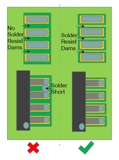
What is a solder mask Dam?
Solder mask dams are spaces between the solder mask relief (this is the edge of the solder mask opening mentioned earlier) of a given solder pad and any adjacent solder pads. Effectively spacing between components.
The purpose of the solder dam is to add further protection from the forming of solder bridges. Keeping some space between components in this fashion is recommended as solder bridges will cause a short circuit and therefore result in a non functioning or incorrectly functioning PCB assembly.
What are some good practices for solder mask when designing my PCB?
When we are reviewing new assemblies for manufacture one of the critical items always checked is the resist windows/solder mask dams.
As we mentioned in the section on PCB pads and tracks/traces; it's important to follow data sheet recommendations for a given component and discuss with your PCB supplier, as often solder resist dams are the first thing to be excluded when a Gerber is panelised.
Remember that a good solder mask is critically important when it comes to producing good production yields. As an example; the simple addition of solder mask dam on fine pitch IC's can prevent very slight process variation resulting in a large number of defective assemblies.
There will be occasions when PCB suppliers cannot apply resist dams due to the distance between the pads. On these occasions it's best to discuss the matter further, often with a little bit of compromise the solder mask dams can be added. For example, trimming some of the width of pads can allow additional space to allow for solder mask dams and this sometimes a better option than going without.
It's always worth taking your time and ensuring a good solder mask layer design on your PCB. Very often a very simple and small sacrifice to ensure a decent solder mask can result in much higher yields for manufacturing. This may not be that important to you for prototyping but the costs in failed yields will increase very quickly if you plan on mass producing your design.

Do You Like What You See?
Join the ranks of satisfied engineers and businesses. Register and quote today!
Register