SAS PCB
Where Quality Meets Innovation in PCB Assembly
PCB Design For Manufacturing (DFM) Tips
Tip 03:
Consider Panel Breakouts
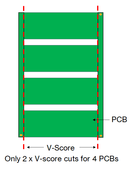
What are panel breakouts?
When a board design is turned in to panels to make mass production easier or if a single board is too small resulting in excess borders; breakouts are included. These are usually perforated sections that allow an assembly to be broken out of the panel once it has been built and assembled, this is known as depanelization.
Breakouts may also be used for when a Printed Circuit Board may be required to fit in to an odd-form space and therefore the design is an odd shape resulting in the need for excess material to be added as is the case for small boards.
An alternative to using panel breakouts or if a small single board is being assembled with no excess borders is to create what is known as a board carrier. This is a separate platform that is custom made for the circuit board to sit on and does the job of supporting it during assembly. The cost of doing so can be pretty expensive so Speed Assembly Services would have to provide this with a manual quote if it is absolutely required but as a general rule of thumb it is something we don’t usually do.
What are the best design practices for including panel breakouts?
It's important to keep components clear of breakout locations, in lower volume manufacture hand tools or nibbler/circular cutters are often used. These require component clearance on the top and bottom of the PCB assembly. Round boards can often cause problems if the gap between PCB and waste is too narrow as it’s difficult to fit straight depanelisation tools into the gap.
V-score if often preferred for PCBs with straight edges and no overhanging components and with clever panel design it can be very quick to break out PCB assemblies.
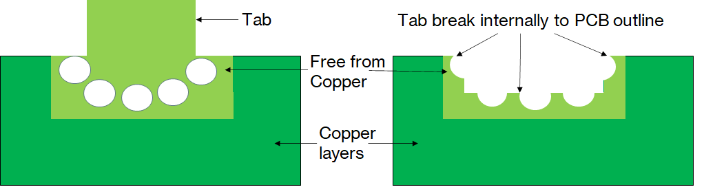
For tab break outs it's worth considering the tab locations in your design if you can. Adding an area free of copper and including the breakout in your design can save time and money. Designing the breakout tab so it breaks internally to your PCB outline can eliminate the need to file or remove burs.
When designing panel break outs it's important to ensure even force distribution to avoid the printed circuit board assembly becoming damaged. We recommend aligning any breaking axis with along each board edge to avoid upward force that may cause damage.
As a general rule of thumb when you are designing break outs you want to avoid creating areas that take an excessive amount of force when the board assembly is being broken out.
A trick you can use to try and help you is to try printing out your printed circuit board design on to a sheet of paper and then fold the paper along each axis of your breakouts. Ideally you want to make sure that none of your folds along your breakouts intersect. If they do intersect then there is a probably chance that this breakout may create uneven force when the board is being broken out.
Do You Like What You See?
Join the ranks of satisfied engineers and businesses. Register and quote today!
Register